Presentation
Presentation
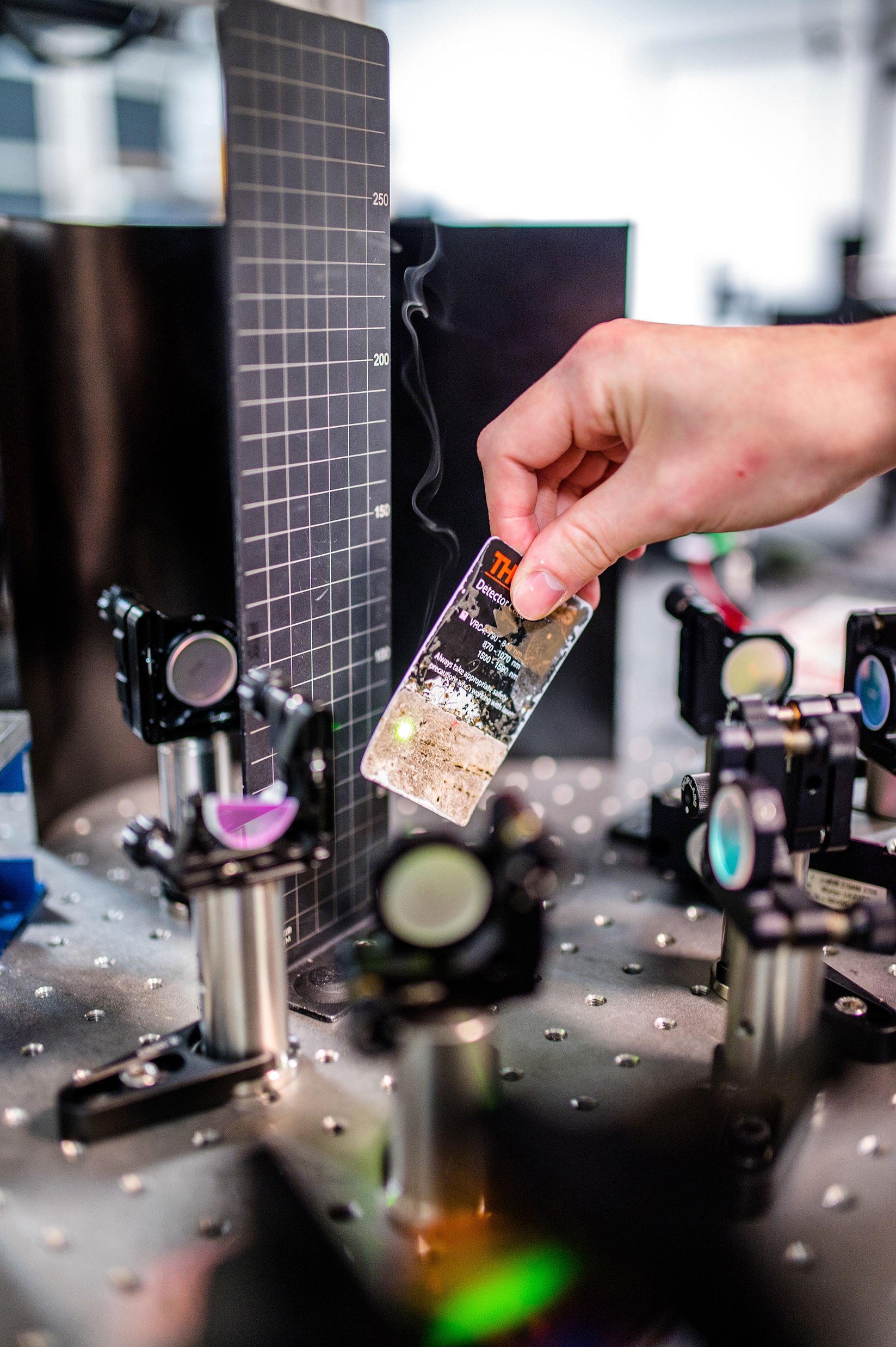
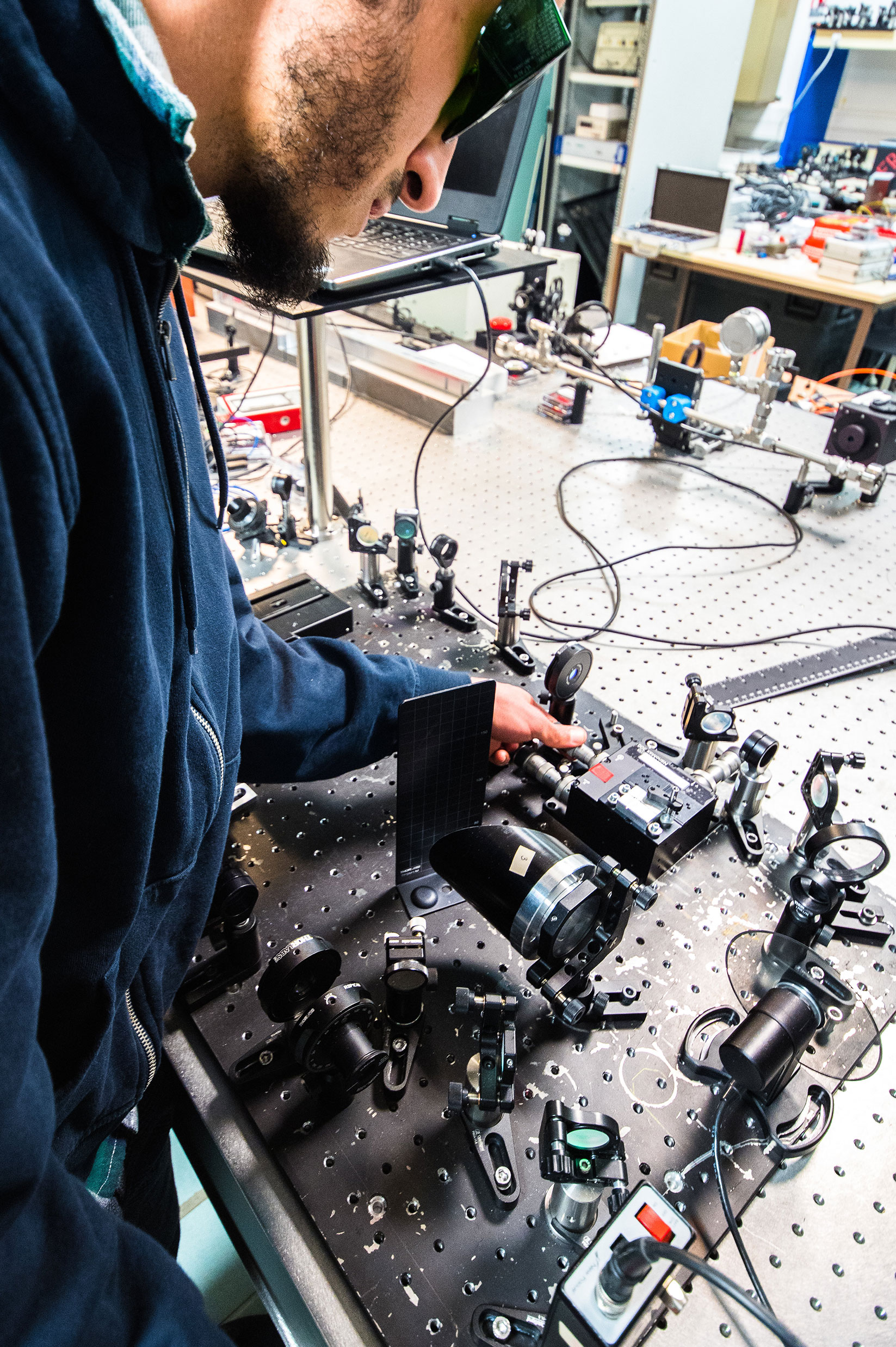
This platform couple optical and electronical means to produce a spatial (2D or 3D cartography) and temporal analysis, of differents sensitivities or characteristics of an integrated circuits. A laser beam is highly focus in differents positions on a chip to induce an photoelectric effect (charge creation) or a non-linear effect but to survey in a non-invasive way the circuit activity.
The platform had 4 microscopes, one horizontal, two verticals and one vertical with reversed column associated toi a test station under tips. On each of those microscopes differents beam can be used in fonction of the wanted interaction and of the semiconductor type. Around each microscopes there is an instrumentation with differents instrument of electrical analysis and circuits polarization, a displacement system of the chip under the beam (step to step platine) or of the beam on the chip (galvanometric scanner). Cooperation betwenn all those elements is automated via a PC IHM developed in C++ or on LABVIEW environment.


